Light can perform calculations: photonics and electronics are changing the way data is processed

From artificial intelligence to data centers, all the way to the devices we use every day, many contemporary technologies are grappling with an increasingly urgent challenge: processing ever larger amounts of data quickly, efficiently, and sustainably. Behind the growth of these technologies there are not only algorithms, but also a very concrete and decisive dimension concerning hardware, energy consumption, and new computing architectures. In this scenario, photonics and electronics come into play: two fields of research that, often invisible to the eyes of those who use computers, networks, and smart devices every day, are becoming increasingly central to the development of the technologies of the present and the future.
To explore these themes in depth, we interviewed Francesco Morichetti, a professor and researcher at the Politecnico di Milano who works on integrated photonics for telecommunications and on the role of light in data processing. Together with him, precisely to recount the value of collaboration among different areas of expertise, Francesco Zanetto, a researcher in the field of electronics, is also taking part. Over the years, the dialogue between their research groups has given rise to a fundamental synergy for the control of photonic chips, for the study of new neural networks and, more generally, for the evolution of technologies that are entering ever more deeply into our daily lives.
Let us begin with neural networks: what are they and what need did they arise from?
FM: Neural networks arose to respond to a need that became central with the spread and growth of artificial intelligence: processing an increasing amount of data efficiently. This need has called into question the way we have carried out computing activities for decades, both at the level of computer architecture and at the physical level of hardware. Traditional computer architecture provides for one part that performs the calculation, the processor, and another that stores the data, the memory: from the laptops we use every day to supercomputers, this is the structure that has become established over the decades.
This structure has limitations when there is a very large amount of data: the exchange between processors and memories can become a so-called bottleneck, which slows down the process. The neural network draws inspiration from the biological world, in particular from the functioning of the brain, where the tasks of storing data and processing calculations are not carried out by different parts, but are distributed among neurons. The neural network is in fact made up of many units that not only perform calculations but also share part of the data.
The world of computing, which today brings computer science, electronics, and photonics into dialogue, is rethinking the classical architecture of processing systems in order to support the enormous growth of data. We researchers are on the front line in studying alternative structures.
Francesco Morichetti, your research group has been working on photonics for some time. How can light be used to process information, thus entering the field of neural networks and, more generally, computing?
FM: To clarify the role of photonics, we need to take a step back from computer architecture and look at its physical part: the hardware.
Processing a large amount of data, as required for example by a supercomputer or an artificial intelligence system, can be demanding above all for three reasons:
- The amount of calculations the system is able to process
- The time the system takes to perform the operation, namely latency
- Energy consumption
Now, it is true that the operations required by artificial intelligence systems are very numerous, but from a mathematical point of view they are often very simple. Most of them, about 85%, consist of elementary operations such as additions and multiplications, which we all learn at school.
This is where photonics comes into play, because we have discovered that photonic circuits are capable of aggregating precisely this 85% of operations, which represents the largest part of the computational cost, thus making the process more efficient.
Was it precisely from these photonic chips that the collaboration with Francesco Zanetto’s research group was born?
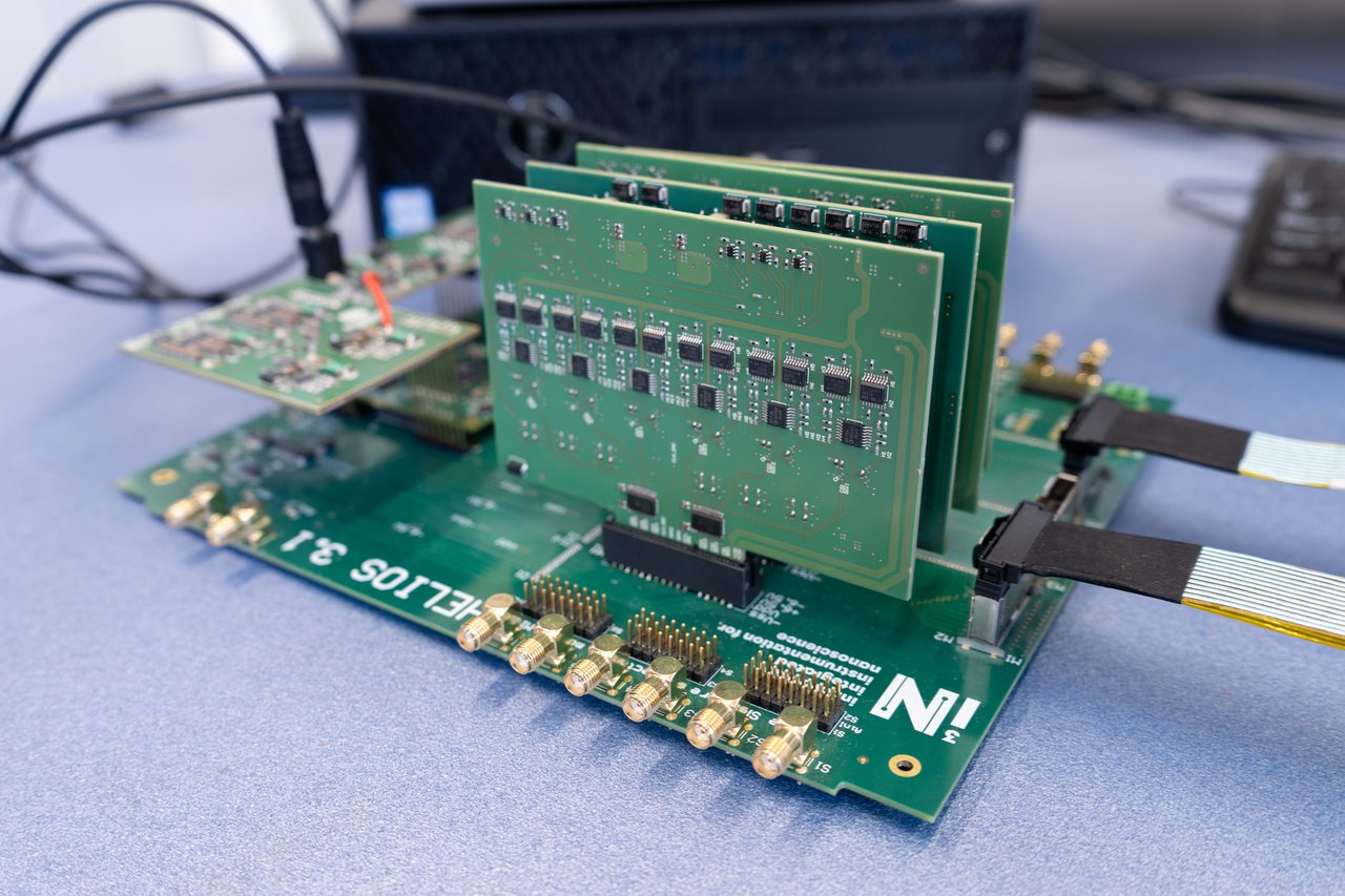
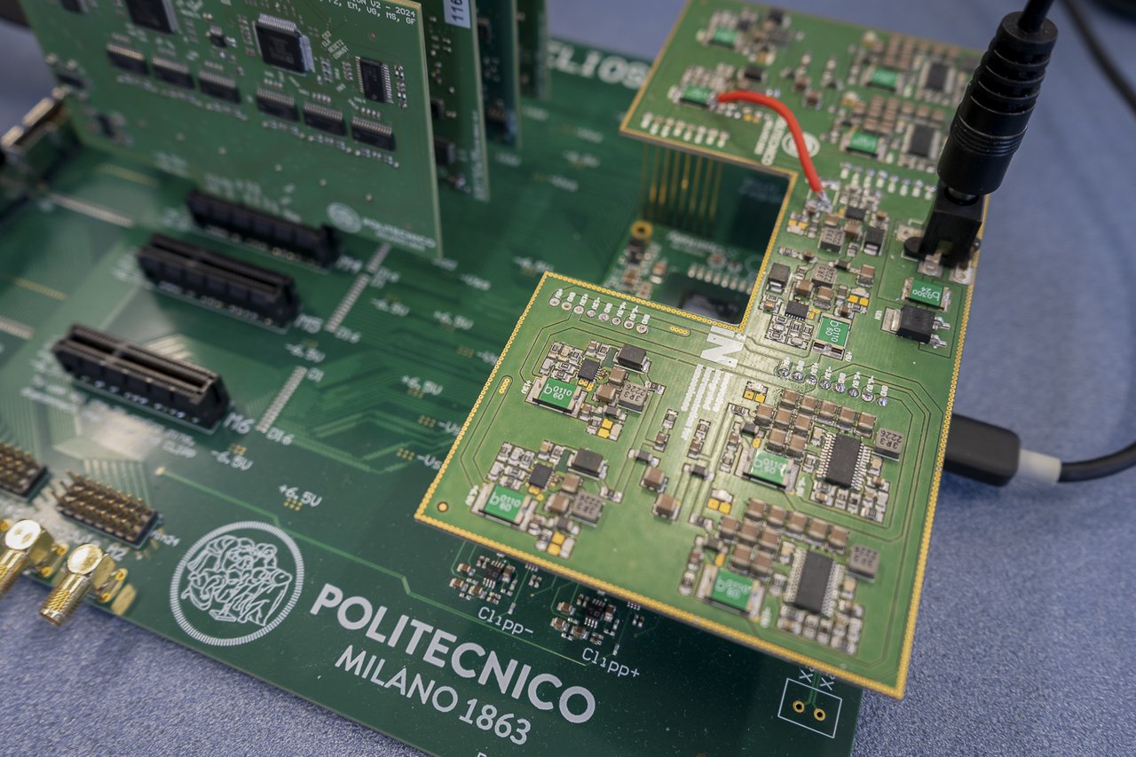
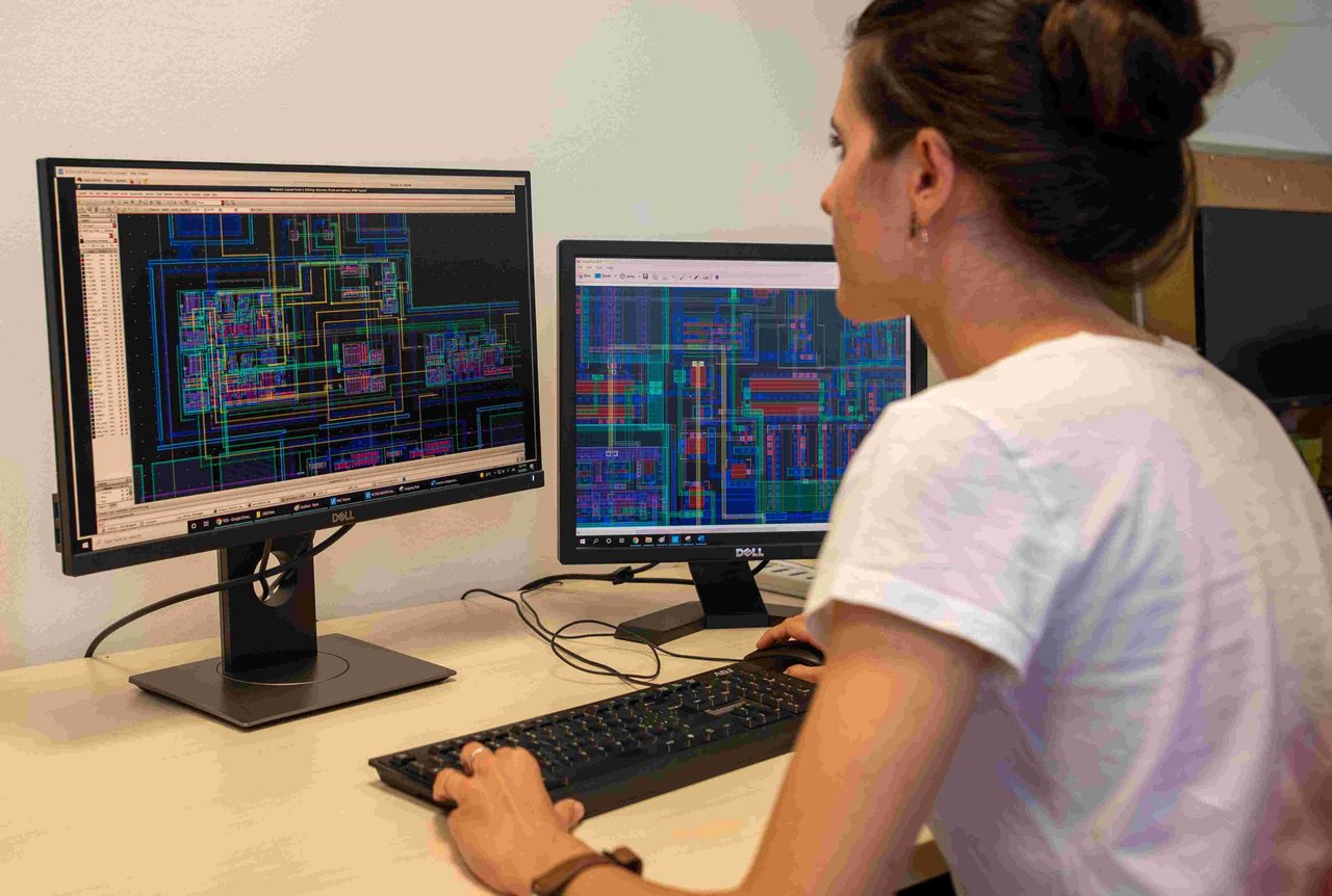
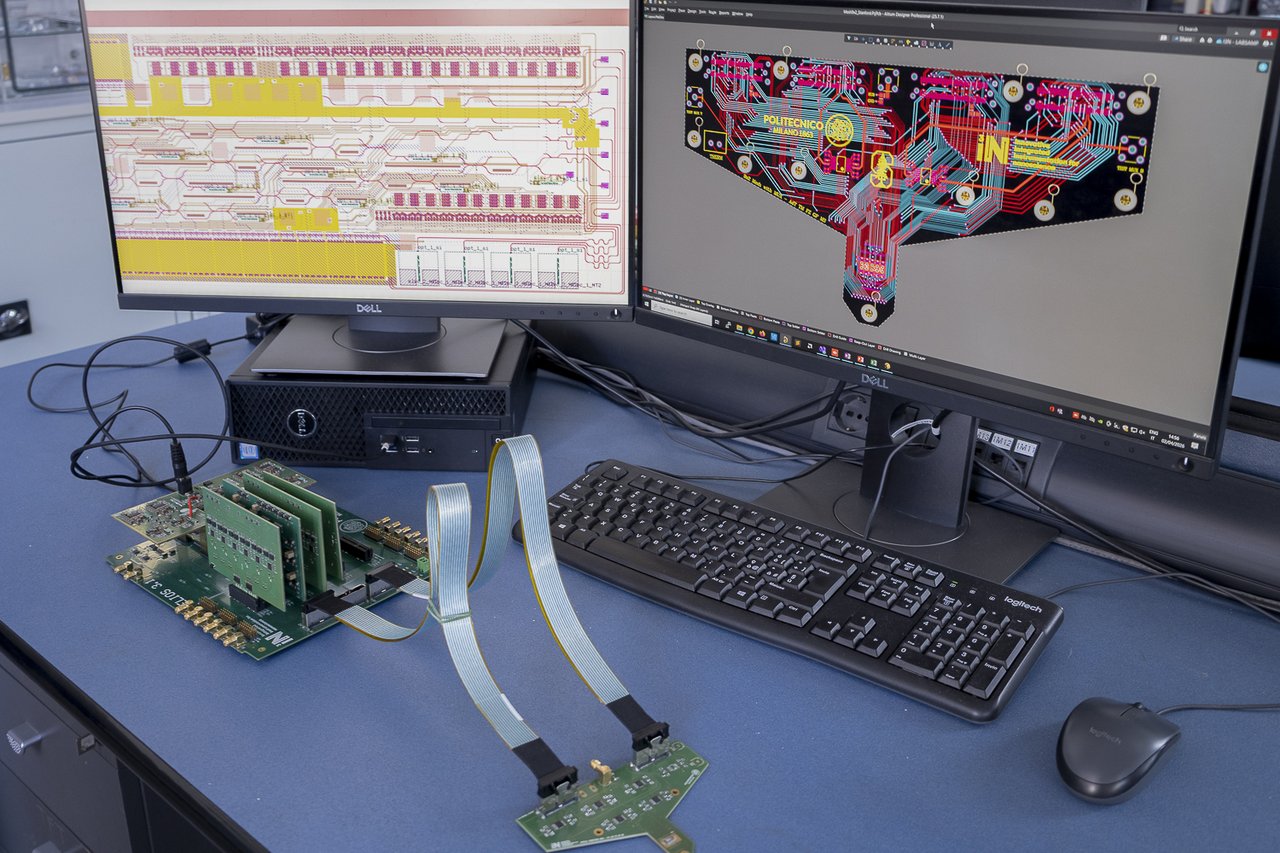
FM: To process light in photonic chips, at least three requirements are needed: knowing how to design them, and today we can do so thanks to increasingly sophisticated design tools; knowing how to manufacture them, and in this sense there are now many foundries that are turning toward photonics; and finally knowing how to “tame” them. This last aspect is particularly important, because photonics needs a control system in order to function well. This is where the role of electronics comes into play, which is what my colleague Francesco Zanetto works on, creating the electronic control systems for our photonic chips.
FZ: One of the most fascinating things about electronics is that it can be placed practically everywhere and can therefore be applied in many different fields, such as photonics. As Francesco Morichetti was saying, tools for design and foundries now allow us to design and build extremely complex objects, made up of basic elements connected to one another.
The functioning of optical devices is not, however, so straightforward. Since they are based on interference between light beams, which is a phenomenon that is very sensitive to imperfections in manufacturing, to changes in temperature, and so on, it is necessary to make sure that the light follows the correct path from the input of the chip to its output. It often happens, therefore, that the circuit can be designed and manufactured fairly easily, but then, once it has been received, the circuit does not work as expected and needs to be calibrated accurately.
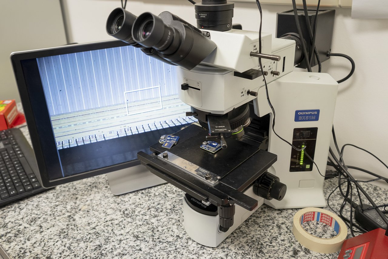
How do we make the optical circuit work in the way we want? First of all, we need to be able to see what is happening at different points in the circuit. For this reason, we disseminate the photonic chip with sensors that can detect how much light is passing through a certain point and, by comparing the measured behavior with the expected one, we drive the actuators that control how interference between the light beams takes place in the circuit.
Until a few years ago, this aspect was less important because photonic circuits were more rudimentary. Now, however, the size of the optical chips we are able to produce has increased considerably, and with it their complexity.
FM: For those working in photonics, this aspect is vital, and collaboration with our colleagues in electronics is fundamental. We can put it with a metaphor: let us imagine a car. Photonics is the engine; it has many horsepower because it is very powerful. But electronics is the control unit, which manages the information coming from the sensors and checks that everything works. Without the control unit, today’s cars would not go anywhere.e.
The study published in Nature to which you contributed speaks of a paradigm shift: neural networks move from the digital to the physical. What does this mean, concretely?
FM: After decades in which digital processing established itself as the technology for computing, today the advantages of a targeted return to analog are being reassessed, and in particular to an approach to computation that directly exploits physical phenomena. To explain this new approach, we can start from a very simple image: the apple falling from the tree. At school we learn to describe that physical phenomenon, linked to gravity, through mathematics. But if a physical phenomenon corresponds to a mathematical model, the reverse is also true: observing and measuring that phenomenon means, in a certain sense, solving the mathematical problem that describes it.
Applied to our field, this means that if the functioning of a photonic circuit is described by a series of mathematical equations, we can design a circuit that physically realizes and solves that problem. In other words, by letting light propagate inside the circuit we can obtain the solution to the mathematical problem simply by measuring the light at the output. The physical phenomenon, in our case the circuit, thus becomes a sort of 1:1-scale mapping of the mathematical problem. This analog approach is gaining ground because some physical phenomena, such as the interference between light beams Francesco Zanetto was talking about, if managed appropriately are also able to solve complex mathematical problems. It is no coincidence that, here at the Politecnico di Milano, last year we launched a course in Photonic Computing, which represents a unique case not only in Italy, but also internationally.
Using analog—light, in our case—offers advantages. What are they?
FZ: Using the interference between two light beams to calculate the product of two numbers means being able to perform operations at the speed of light: going faster than light is decidedly difficult! In addition to being faster, analog neural networks also manage to consume less energy. Making a photon travel along an optical fiber or inside an optical chip is relatively easy and does not involve dissipation of energy along the path.
At the moment these aspects are being studied, but the results are promising and the progress we have been observing in recent years is very rapid. Our vision is that in a short time, five or ten years at most, these technologies may enter the computing units of supercomputers and data centers, assisting the neural networks used for artificial intelligence, with evident benefits in terms of energy consumption, and therefore also from the point of view of environmental impact.
Another advantage mentioned in the study, in addition to reduced consumption and increased speed, is the possibility of processing calculations in situ, without having to transfer the data elsewhere. Why is this important?
FM: Transporting data from one point to another costs energy. This is why, at this moment, inside all the supercomputers and all the data centers in the world the connections are already in optical fiber. As Francesco was saying, moving light, that is photons, costs much less than moving currents of electrons. Optical fiber is therefore already used for transporting data: data centers are nothing other than cabinets containing server units connected to one another thanks to optical fiber.
The further step that one would like to take is to bring optics further inside server units, thus reducing the distances that have to be covered electronically. Exchanging data as much as possible in situ, making the process happen close to where the data is stored, is the direction in which the neural network is moving. Since last year there has been a great deal of talk about co-packaged optics: electronics and photonics, which used to be in two separate devices connected to one another, are now placed very close together inside the same package.
FZ: If we use it not only to transmit the data but also to process it directly, we reduce the conversions from the electrical domain to the optical one, which are the aspects that typically require the most energy. The objective is therefore to develop a single compact object capable of processing data directly in situ.
How did the collaboration between your research groups begin?
FM: Our collaboration arose almost by chance, more than ten years ago, when Francesco Zanetto was probably still a student. It all began in front of the coffee machine, where I met Prof. Marco Sampietro, who works in electronics. That day he was particularly satisfied because he had obtained a very important result in his field: he had managed to measure a very tiny variation in an electrical parameter, something no one had ever managed to do before. We in the photonics group did not let the opportunity slip by and immediately threw him another challenge: detecting the passage of light inside an optical chip without extracting photons; therefore, in a totally non-invasive way and different from what is normally done. In a few weeks—truly in record time—our colleagues managed to do it using their electronic technology!
At that moment we understood that our office neighbors had the skills to support our research activity; at the same time, they saw that electronics, among its many possible applications, could also find important space in photonics. From there began a collaboration that has lasted for almost fifteen years and that has led to a great many shared high-level scientific publications. I think the synergy that has been created is rare, almost enviable: it is not common, in fact, to find within the same university such highly specialized expertise capable of working in such an integrated way. Or very probably there are others here at the Politecnico, but these virtuous short circuits have not yet been created.
FZ: As the saying goes, eating comes with the appetite. We started with relatively simple tests and, since they worked, our colleagues immediately pushed us to take one step further: since we had succeeded in that first challenge, we could try to tackle a more complex one. We went on like this, continually relaunching new challenges to one another. This mutual stimulus allowed us to grow and evolve. I completely agree with what Francesco was saying: it is one of our strengths. The synergy that has been created runs through all levels of the project, to the point that today we design the optical circuits together in order to obtain a result that works as well as possible and meets all the requirements.
So an important collaboration, founded on highly specialized and complementary skills. What research projects are you involved in together today?
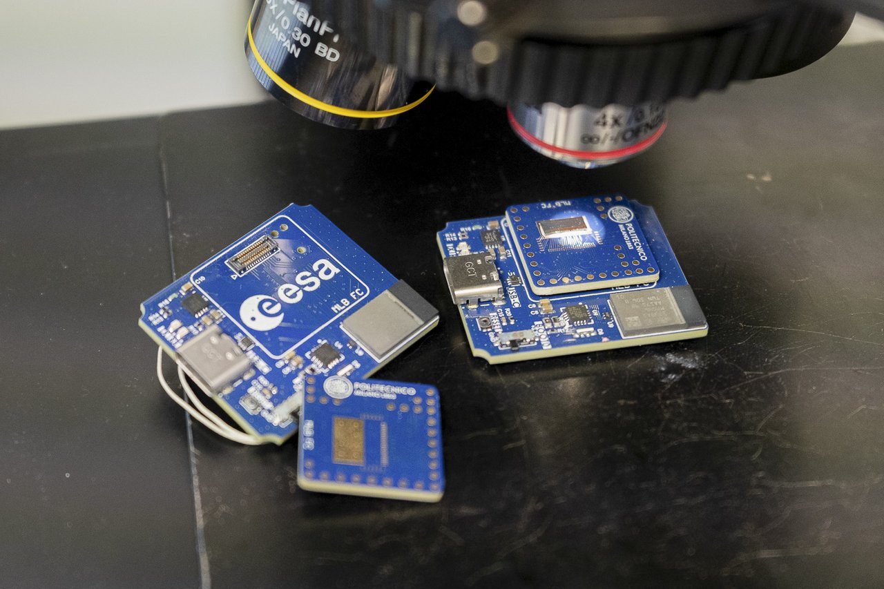
FM: We are currently involved in two major European projects linked to the Chips Joint Undertaking (Chips JU), the European Union instrument that, within the framework of the European Chips Act, supports the development of chip technologies, including photonic ones. These are two pilot lines, that is, initiatives designed to strengthen and make the entire integrated photonics supply chain more mature, bringing research closer to industrial adoption. In this context our contribution concerns the control, calibration, and testing part, which are essential aspects to make these systems work reliably, especially when they have to operate in an operational environment, that is, outside a research laboratory. It is work we have been carrying out for years and that today is beginning to yield very significant results because our expertise is recognized internationally.
This technology is very promising, but it does not yet seem to have completely come out of laboratories. What steps are necessary to arrive at a more widespread application?
FM: First of all, it must be borne in mind that integrated photonics was born in the 1990s, about forty years later than electronics. Until some fifteen years ago, in many cases it remained a wonderful research topic, at times an academic exercise, because real large-scale applications were lacking. Today, however, the sector has exploded, above all thanks to the artificial intelligence market, which continues to grow and which, precisely for this reason, urgently raises the issue of sustainability.
Data centers have reached energy consumption levels comparable to those of medium-sized cities. To give an idea, a traditional large-scale data center can require between 20 and 100 MW of electrical power, the equivalent of a city such as Novara. But it is thought that the new sites dedicated to artificial intelligence may even reach powers ten times greater, so much so that in some cases power plants have been built nearby to supply them. If artificial intelligence models continue to grow, as everything suggests they will, we will no longer be able to reason according to the traditional paradigm: it is not enough to increase the number of processors in order to handle ever larger amounts of data.
In recent years, large industries once active exclusively in microelectronics have begun to invest in integrated photonics. Volumes are still limited compared with those of electronics, but they are growing rapidly. A virtuous circle is thus triggered: as volumes increase, investments also grow, which in turn accelerate development times. Today we can no longer afford to wait twenty years to have an alternative or complementary technology to the current one.
The real challenge is to achieve a level of technological maturity such as to bring laboratory prototypes toward engineering and then industrialization. It is a step that fits fully within this paradigm shift. A parallel can be drawn with electric cars: for years they remained a distant prospect, then a series of technological and market transformations accelerated their development.
FZ: One of the key points for industrial scalability is precisely the aspect we are working on: control, which becomes increasingly complex when chips no longer contain just a few functional units, but thousands. To put a product on the market, it is not enough for it to work well: the real challenge is to ensure that its performance remains stable over time, at the desired level. This is the leap that is taking place now: if until recently getting an ambitious technology to work even for just a few minutes was already a result, today the goal is to obtain reliable performance for much longer periods, potentially years.

Let us delve into the synergy between electronics and photonics. Do you think hybrid systems will play an increasingly central role in the future?
FZ: There are already companies that produce hybrid chips, in which a photonic component and an electronic one coexist. The two domains, in fact, integrate very well. So far we have spoken mainly about optical circuits, which are analog systems and which, to be regulated correctly, need an electronic control unit capable of keeping them under control.
But this is not the only application in which electronics and optics work well together: another fundamental field is information transmission. As we have seen, the most efficient way to connect two points separated in space is optics. To do this, however, circuits are needed that convert the signal from electrical to optical, and electronic devices capable of driving the optical components that make information transmission possible. I therefore believe that, in the future, this synergy will become increasingly close, because it offers very concrete advantages in terms of speed and energy efficiency.
FM: I think the winning strategy is to use electronics for what it does better than photonics, and vice versa. In the past there was much speculation about the potential of photonics, especially in the early 2000s, when the advantages and limits of photonic technologies were not yet well understood. The enthusiasm was such that people even imagined an entirely photonic computer, without digital processors. It was, however, realized quite soon that this hypothesis did not hold: photonics still needs an electronic component for control and supervision. And in any case it cannot entirely replace digital processing.
Hybrid systems therefore represent the most effective solution. In this sense, the nature of materials also helps us: silicon, which is the fundamental material of electronics, is also excellent for photonics. On silicon chips we can therefore combine the advantages of both. Naturally, between saying it and doing it there has been a long development effort, but today some industries are already able to fabricate on the same chip an electronic part and an optical part, with an approach we define as monolithic, because it is built on the same material substrate.
Let us keep our gaze turned toward the future. Which research frontiers seem most promising to you today in your field?
FZ: The field that today makes the greatest use of optics is that of data communications, and I believe its use in this sector will continue to grow in the future as well. At the same time, I think that optics will increasingly be used both for computing and for sensing the environment in which the system operates. Just think of the optical fiber cables that cross the oceans: if appropriately equipped with sensors, they could be used to detect earthquakes or to understand what is passing through a given point, for example a whale or a submarine.
FM: Francesco stole my answer! The direction in which we are moving is that of communication and sensing in many different fields. Autonomous vehicles, drones, robots, and wearable devices, such as smart glasses, are all objects that in some way have to “look around” and, at the same time, communicate. To do both they need many sensors, for example to measure the position, distance, and speed of surrounding objects. The chips we make are able to use light for this as well, and this makes them potentially excellent sensors, capable of detecting even very small changes in the environment.
Francesco Zanetto, how did you come to research in the field of electronics?
FZ: For me it was almost the result of chance. Along my path I saw that, with the right commitment, we were able to achieve very good results, and this motivated me a great deal. Everything then continued quite naturally: every step forward we managed to make opened up the possibility of taking another. Sometimes one does not fully realize the importance of the results achieved; one understands it above all when speaking about them with someone else and perceiving their amazement or enthusiasm. This too is a strong stimulus to continue in the direction undertaken.
Francesco Morichetti, how did your research path in photonics develop?
FM: If I think about it, my path has been coherent from the very beginning. I studied telecommunications engineering here at the Politecnico and became passionate about optical communications and light very early on. I continued along this path, even though various contextual events could have led me to reconsider it: I graduated in 2001, just when the telecommunications bubble burst, until then a sector in full development and rich in investment.
Faced with that crisis, I had to find the motivation to continue my research beyond the logic of the market. I remember that, in those years, at sector conferences some people murmured that integrated photonics was already dead, less than two decades after its birth. We, however, continued to work on optical chips, above all silicon ones, with great determination, because we liked what we were doing and because, deep down, we believed in it.
Now almost twenty years have passed and we see that interest, including industrial interest, has been rekindled more strongly than before. But today’s results are the fruit of the work and study carried out then to do science and produce knowledge. In that period we received only funding from ministries and from the European Commission; today our research is funded by a growing number of industries entering the sector. With hindsight, we can say that we did well to hold firm. In general, I think it is important not to let oneself be overly conditioned by the fashions of the moment and, when one truly believes in something, also to have the courage to work against the tide.
What lines of research would you like to work on in the future?
FM: One field that I find very interesting is biosensing, that is, those devices that are little or not at all invasive and are used to detect biological parameters. Letting my imagination run a little, I would like to work on chips integrated into smartwatches or even under the skin. In the past we had the opportunity to tackle a few projects in this field, but we did not have the time and resources to devote ourselves to it in depth. I believe there is still a great deal to do and to experiment with here. Francesco, have you also worked on something in this field?
FZ: Yes, and it is a very complex field, because it requires expertise in chemistry and in particular in biochemistry. From the outside it may seem simpler than it really is. I too find it very interesting, fascinating, and far from trivial.
As for me and our laboratory, what we are most passionate about is being able to measure something that is difficult to measure. This interest takes shape in photonics, but also in many other fields, such as environmental monitoring, quantum computers, or biology. Any challenge of this kind is welcome, because for us it represents a strong stimulus.
FM: Another very interesting field is space. In the past we carried out research activities on the resistance of photonic chips to ionizing radiation, successfully passing the tests. Space is a hostile environment, so devices must be tested with respect to exposure to high doses of radiation. Today interest in this sector has grown and I think it would be very stimulating to work on sensing, monitoring, and communication components. Knowing, for example, that a satellite equipped with our chips has been launched into space would be an enormous emotion, and we are also equipping ourselves in this direction.
What would you recommend to a young person who is passionate about your field of research?
FM: I think that outside academia, especially among young people, there is a somewhat distorted view of the needs of the field of information technologies. Today the whole world is moving in the direction of machine learning and artificial intelligence. In this process, however, there is often a tendency to consider only the algorithmic and software component of technologies related to artificial intelligence. But we must not forget that what has really made the difference is hardware. Many algorithms had long been known; what made the large-scale operation of artificial intelligence systems possible was the evolution of computing hardware, which today makes it possible to implement these algorithms effectively.
However, industries operating in hardware struggle to find people ready for the world of work with skills in electronics and photonics. Students and PhD candidates with this profile are becoming increasingly valuable. In part, I believe this also depends on a prejudice against disciplines perceived as more traditional. But it is important to remember that today’s electronics is very different from yesterday’s, and photonics did not exist yesterday.
The loss of expertise in this field is not only an Italian phenomenon, but also concerns Europe and North America. Initiatives such as the Chips Act are aimed precisely at bringing back expertise and infrastructures that are now more concentrated in other areas of the world. Let us not forget that chips are a strategic resource: in some ways, the oil of our century, and whoever controls their production holds a great lever of power.
You might also like
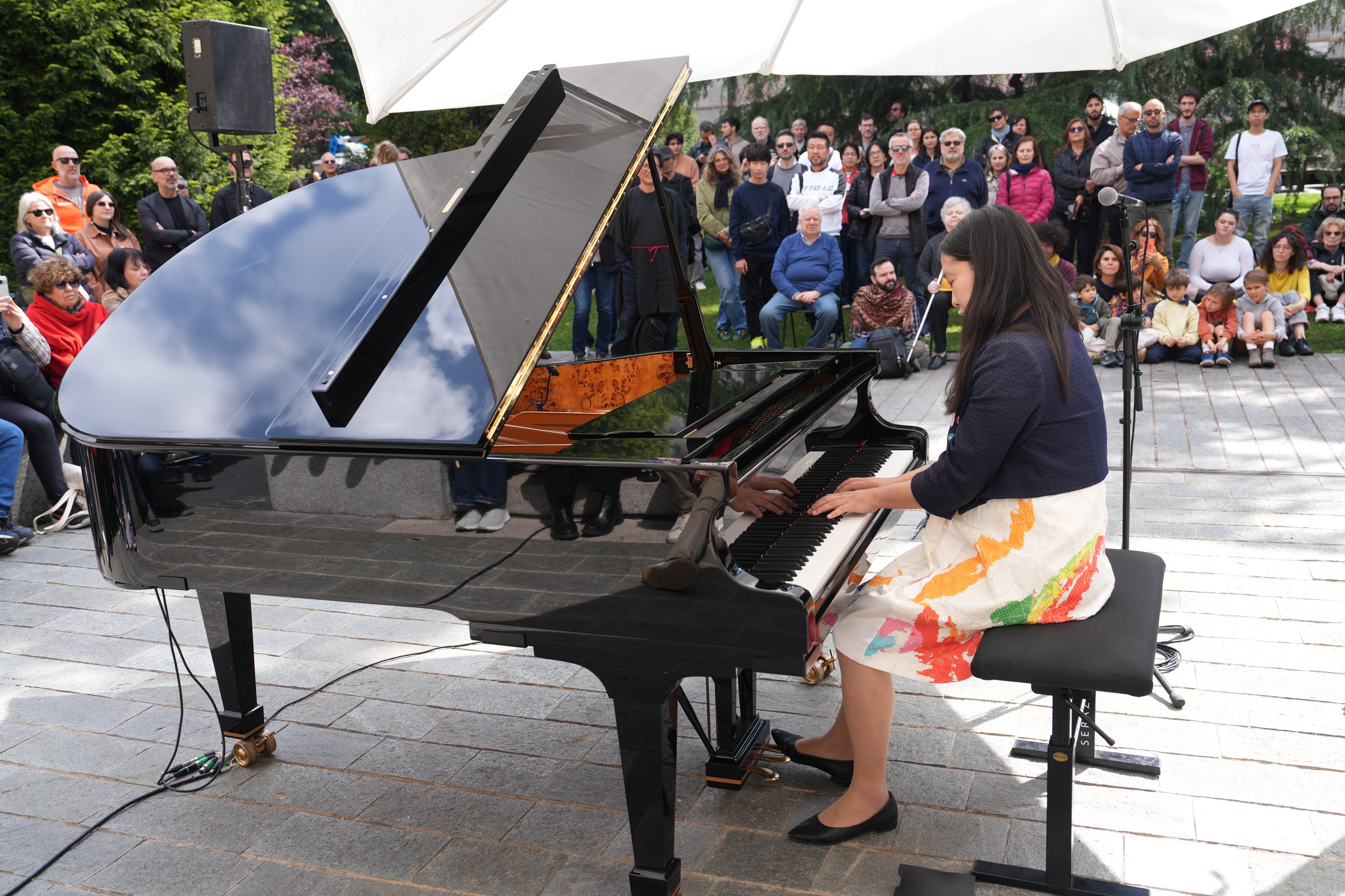
The creative force of mathematics, in the words of Sachiko Nakajima
The scientist and pianist is a tireless promoter of topics such as STEM, diversity and inclusion. In this interview she told us about her artistic world and her vision of mathematics.
Circular Fashion-Tech Lab: where fashion becomes truly circular
Integrating design and advanced technologies from a more sustainable perspective

Architecture is not architecture: Ma Yansong's lecture

Where design engages with living matter: B.Lab and the future of biodesign
The human being as part of an ecosystem. B.Lab, the new laboratory at Politecnico di Milano dedicated to biodesign and materials for transition, originates from this shift in perspective. Among mycelia, algae, bacterial cellulose and waste biomasses, the…