2Exciting is new, but is already thinking big. An innovative training network for a new generation of scientists with the highest nano-optoelectronic skills. The project was so ambitious that it was awarded a €3.92 million budget for being ‘Innovative Training Network‘ by the Marie Skłodowska-Curie Actions.
The European H2020 Programme named after the great scientist, Marie Skłodowska-Curie, instituted several international actions to develop training networks and mobility programmes. ITNs are innovative networks for training a new generation of creative, entrepreneurial, and innovative researchers capable of facing current and future challenges.
The network is coordinated by TU Dresden’sProfessor of Theoretical Chemistry Thomas Heine. Taking part are eight academic groups from among leading European players in the field of two-dimensional semiconductors [2DS] and eight high-profile companies to train 15 early-career researchers in scientific and transverse skills.
At Politecnico di Milano, the project representative is Christoph Gadermaier from the Department of Physics.
Professor Gadermaier could you define nano-optoelectronics?
Optoelectronics covers technology that combines electronics and light, for example, in the displays on our mobiles and computers. ‘Nano’ relates to sizes ranging from 1 to 100 nanometres (from a millionth to ten thousandths of a millimetre).
How do you work on such a small scale?
The current production of optoelectronic devices starts with a block of semiconductor, which is sculpted into smaller structures. Nano-optoelectronics uses materials that provide the constituent elements of nanometre dimensions. Many optical and electronic properties change at such small scales compared to larger structures made from non-nano variants of the same materials.
Our project, 2Exciting, relates to a class of nanomaterials that interact strongly with light, which means that we can achieve small scale optoelectronic functionality.
What are nano-optoelectronics current challenges?
There are two energy problems associated with electronics. The first is electricity consumption and the other is that it is used inside small devices, which means heat is a performance stumbling block.
How are you meeting these challenges?
Light can be more energy efficient than electricity. This idea was introduced decades ago with fibre optics in transatlantic cables and has led to the internet connections in our homes and offices. We can apply the technology over shorter distances, like between computers within a data centre, but it doesn’t end there.
What do you envision for the future?
The next steps will be optical communication between the chips in a computer or mobile phone and then the components on the same chip. Nano-optoelectronics translate an electronic signal into an optical signal and back in a nanometre-sized device.
What are your laboratories specialisations ?
Our group in the Department of Physics studies the fundamental processes that develop such devices.
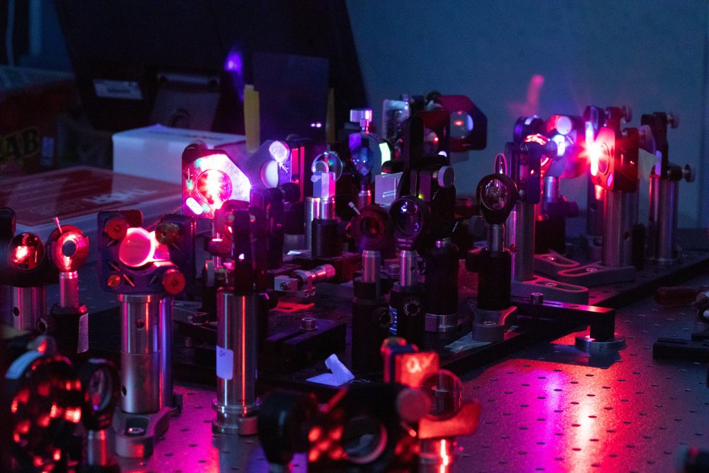
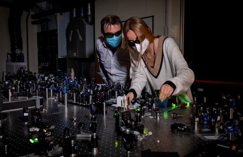
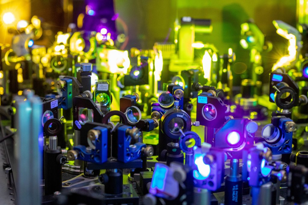
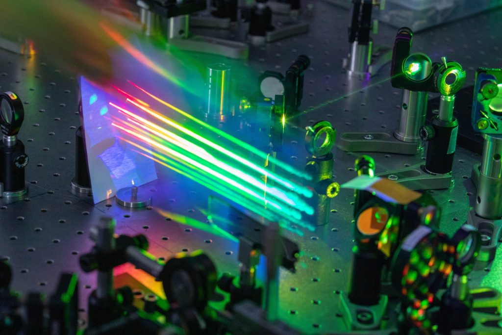
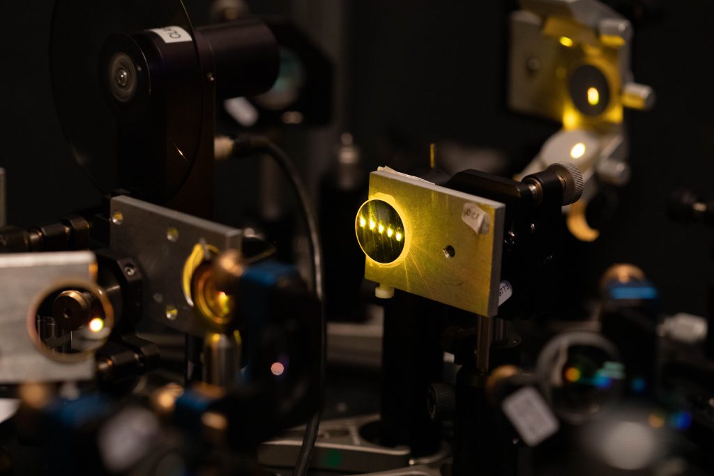
Many of these processes are extremely fast, so we cannot measure them with electronics. Instead, we measure them using short laser pulses with a technique we call ‘ultrafast transient absorption’, which is unique to our laboratories.
The project seems to have broad implications …
While our project focuses on optoelectronics, the basic physical processes when an optical signal is converted into electronics are the same as solar energy being converted into electricity. The importance of our results does not stop at electronics, but extends to what is called ‘light harvesting’: photovoltaics and photocatalysis and primarily the production of green hydrogen.
Gadermaier helps us understand how the science of optoelectronics and two-dimensional materials forms the backbone of the Internet age, and will be a fundamental part of Europe’s economy and security in the future. Europe is in a good starting position, but there is a lack of highly qualified researchers and developers with experience in this field.
This is where the 2Exciting network comes in. It provides an incredibly valuable opportunity to train the next generation of scientists in such an important and strategic area. The new network offers a type of training that combines scientific skills and complementary abilities. Young researchers will study the fundamental physics of light-matter interaction in 2DS to develop innovative optoelectronic devices for telecommunications and next-generation technological applications.
The training programme, comprises three winter schools and three satellite events. It provides scientific and industrial training for network researchers, and involves instructors from non-academic partners, dealing with technological issues and complementary skills such as technology transfer, entrepreneurship, and dissemination. A crucial element of every young researcher’s experience is the chance of a six-month inter-sector and international exchange.
One of these young researchers is the Irantzu Landa Garcia, a graduate of the Universitat de Barcelona who has just enrolled in the 36th cycle of the PhD in Physics as part of the 2Exciting project.
Irantzu, what are your research goals?
The project’s main objective is to gain a deeper qualitative understanding of the electronic processes of two-dimensional semiconductors. The goal is using the photophysical and optoelectronic properties of these promising new materials for technical applications in 2D optoelectronics. We would like to control their electronic structure with external means.
How do you do that?
The research focuses on studying the role of deformation, defects, and the dielectric environment on the electronic dynamics of materials. By externally controlling the electronic structure, we introduce a tool that could regulate and improve the optoelectronic behaviour of functional two-dimensional semiconductor devices.
What do you hope to gain from your Italian experience?
I would like to develop my personal career as a researcher, become a specialist, and develop new skills in a field of research that aims to answer questions that interests me. This is why doing research here is an extraordinary opportunity, since I am working with experts in the field who work remarkably, with excellent infrastructure and laboratories.
And on a personal level?
I am sure that doing my PhD abroad will be a unique experience, for my research and on a cultural level. New perspectives and views of the world can enrich me personally and my career.