Ten years ago, at the Politecnico di Milano, Polifab was born, the large university infrastructure that hosts state-of-the-art instruments and equipment in the field of micro- and nanotechnologies. The idea was to create a shared, accessible, and technologically advanced space, capable of overcoming the limits of individual departmental laboratories.
It was conceived, among others, by two Department Directors, Gian Antonio Magnani and Rinaldo Cubeddu, together with the then-rector Giovanni Azzone and Donatella Sciuto, the current rector. Polifab was designed as a laboratory at the service of academic research that was at the same time capable of dialoguing with companies in the territory.
Today, Polifab is a consolidated reality, frequented by students, researchers, startups, and companies, and involves five Departments of the Politecnico: Physics; Electronics, Information and Bioengineering; Civil and Environmental Engineering; Mechanical Engineering; Chemistry, Materials and Chemical Engineering. In 2024, more than 160 doctoral candidates, researchers, and professionals from companies and startups had access to Polifab. Over twenty companies regularly use the services provided by Polifab. The results speak for themselves: collaboration with companies has generated projects, products, and new ideas—many more than were expected at the beginning
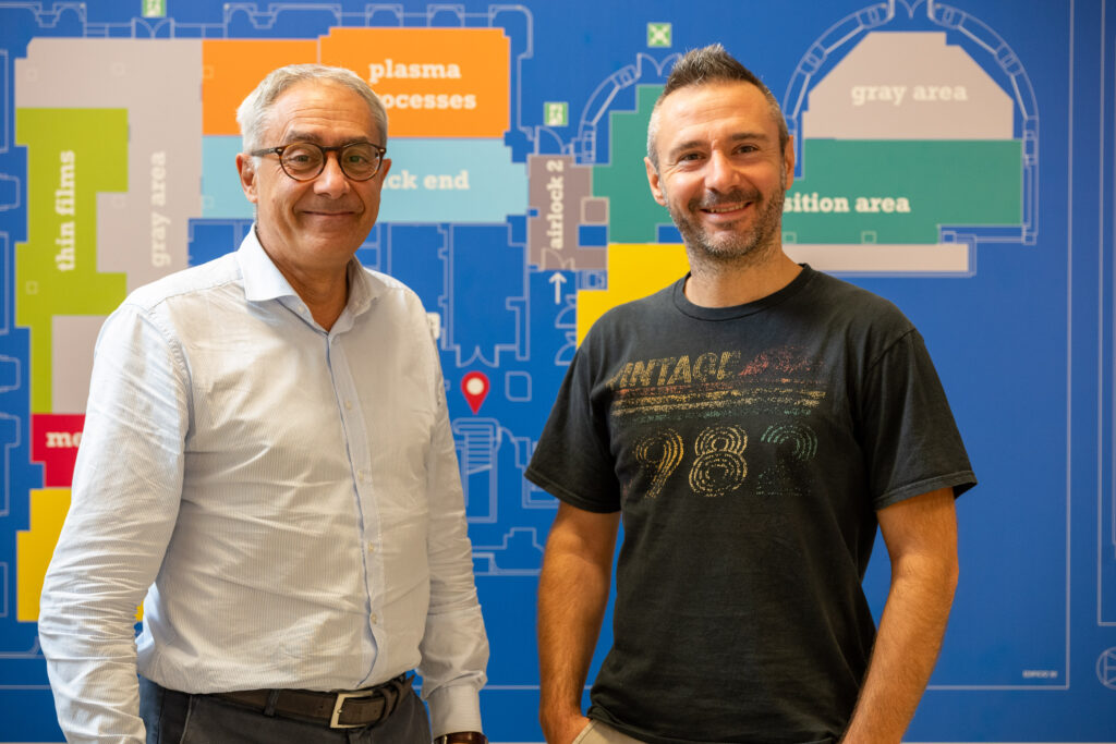
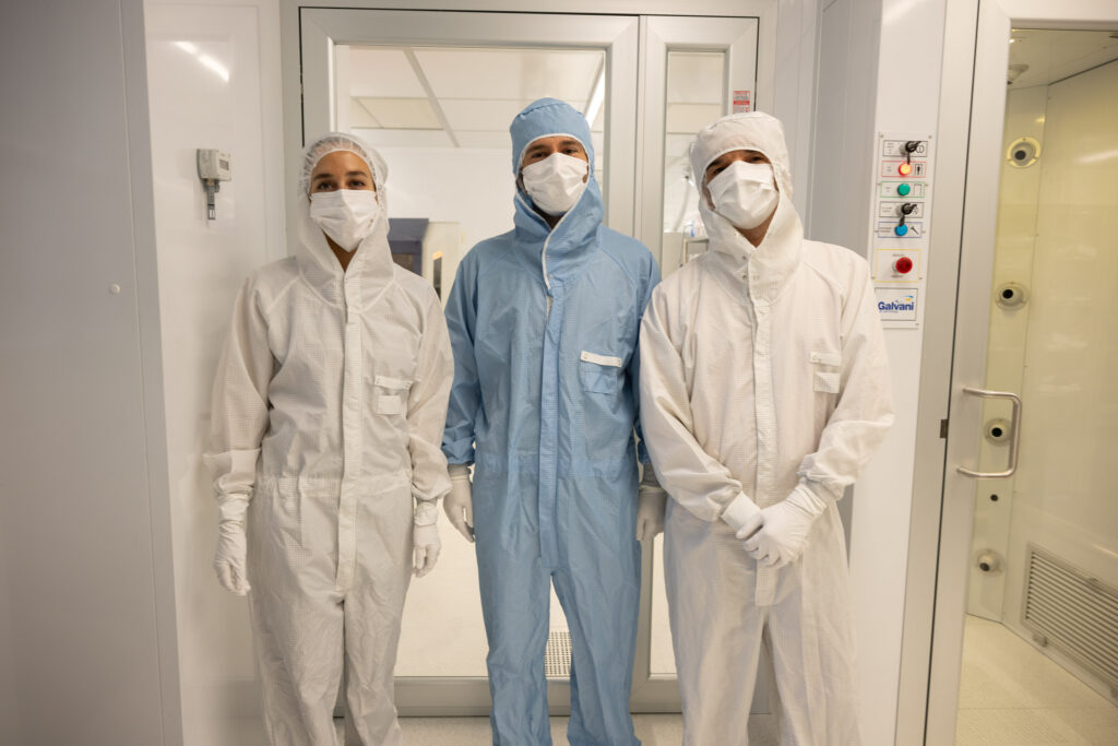
We met Andrea Melloni, Director of the Scientific Committee of Polifab, and Claudio Somaschini, the structure’s manager. Together with them we entered one of the most unique places at the Politecnico: the cleanroom.
The cleanroom: the heart of Polifab
But what is a cleanroom? Also called a “white room,” it is literally a “clean room.”
In the field of microelectronics and semiconductors, the problem is not so much microorganisms as the dust present in everyday environments. When devices are built on a nanometric scale, even a grain of dust can be a mountain. Therefore, if a dust particle settled on a device so small as to be invisible to the naked eye, it would compromise its functioning.
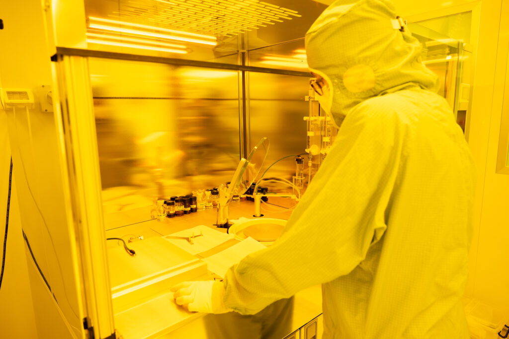
Hence the need for a place with an extremely low particle count. The first cleanrooms were born in America in 1960, alongside the birth of modern microelectronics.
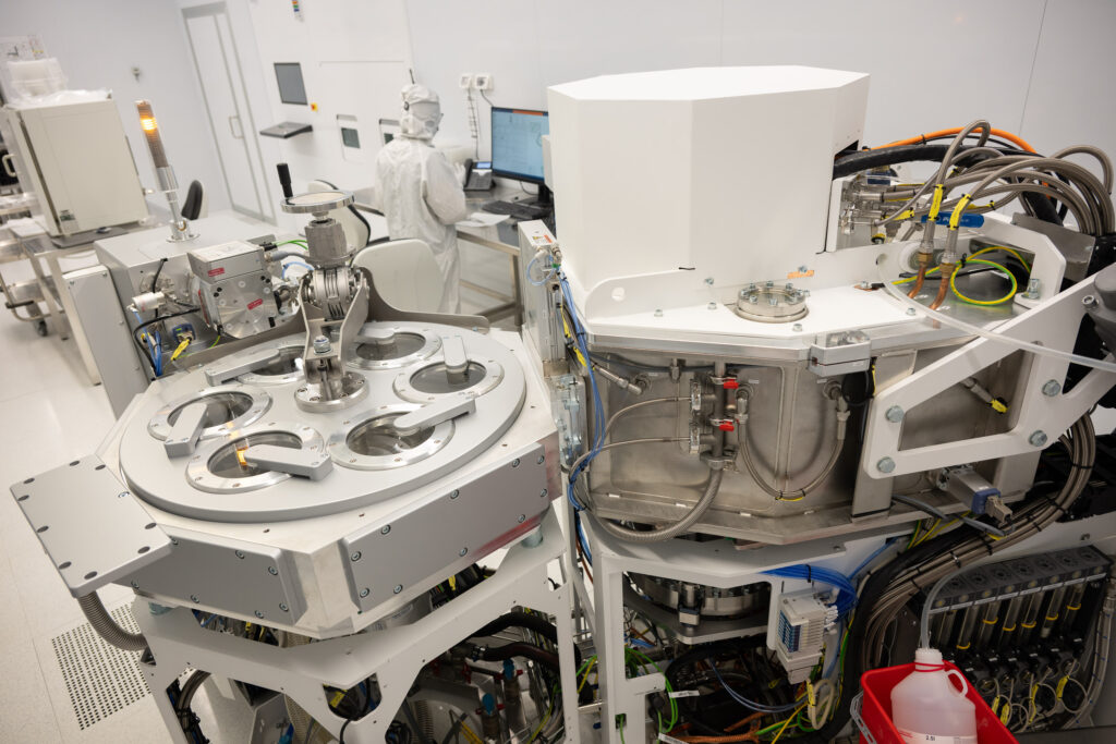
To guarantee a controlled environment, the cleanroom is crossed by constant flows of filtered air and its rooms are maintained at positive pressure, the air from inside the clean room is forced to go out and halt the dirty air. At Polifab work is done in ISO Class 6: an intermediate level of cleanliness compared to industrial standards, but ideal for university research.
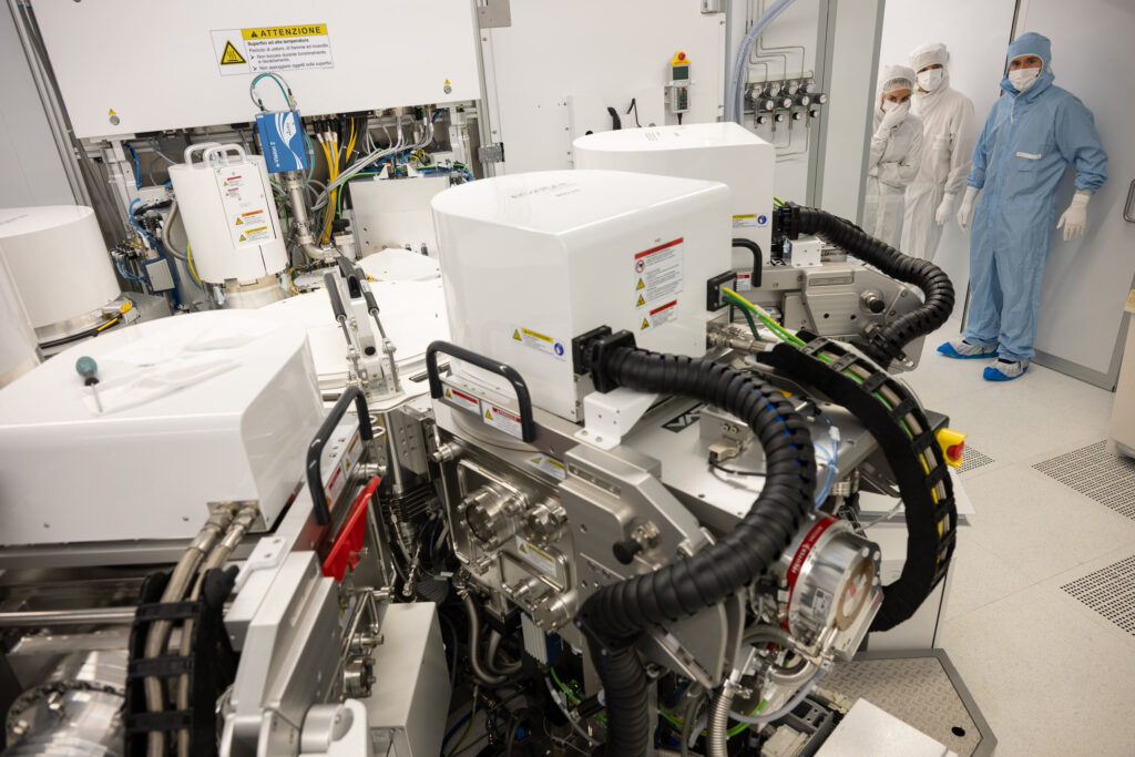
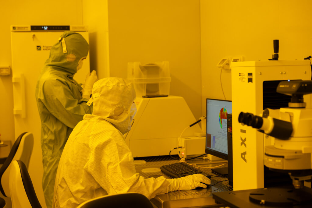
The great advantage of having a research infrastructure such as a cleanroom at a university is that laboratories from multiple departments gravitate around it. Researchers can thus produce very small electronic devices and bring them to other laboratories for testing and use for their intended purposes. For example, sensors and actuators are developed using innovative piezoelectric materials, microfluidic devices for medical purposes, and nanostructured metasurfaces for optical applications.
An open laboratory
Thanks to Polifab, university professors, students, startups or large companies could now have a better access. Here enter students, PhD candidates, researchers, and professors from the Politecnico, as well as external users from research centres and other universities. Five degree programs at the Politecnico use Polifab for teaching activities, offering students the opportunity to “learn by doing”. It is not uncommon for a thesis project to turn into a passion or a career.
At Polifab, groups work on very different fields of research, from photonics and electronics to the study of new materials. Bringing them together in one environment has enormous value for research multidisciplinarity: it means ideas circulate more easily and quickly, creating opportunities for collaboration.
Polifab is also a reference point for startups and companies, which find here infrastructures and expertise hard to find elsewhere. In some cases, Polifab has succeeded in technology transfer, because some company-commissioned research has become projects put into production. Moreover, Polifab is a place where companies have the opportunity to meet students and PhD candidates who have had direct research experience in the cleanroom. In the ongoing relationship with Polifab, companies thus gain significant value in terms of personnel, knowledge, ideas, and much more.
Research applications at Polifab
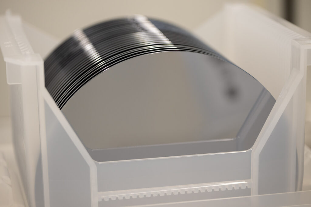
Polifab’s cleanroom was not conceived to serve a single application, nor has it ever been limited to doing so. Everything starts from wafers, slices of silicon on which infinitesimal objects are built—objects invisible to the naked eye but essential for the functioning of advanced electronic devices.
One of the most relevant research areas is that of MEMS (Micro-Electro-Mechanical Systems), of which STMicroelectronics is among the world leaders. But it is not the only field of research because MEMS are electronics tools, already in use. Electronics is now everywhere, and Polifab is able to contribute to the most disparate fields of use—environmental sensors, medical devices, telecommunications, automotive, etc.
When it was inaugurated, Polifab was defined “the workshop of the 21st century”. The beauty of this workshop is that it does not always produce the same thing. This variety is a source of cultural and scientific wealth. Here people with different skills, experiences, and objectives meet. Polifab thus becomes an innovation ecosystem, from which new synergies are born and, often, start-ups that take shape from a shared insight.
Collaboration with STMicroelectronics
TAmong the most important collaborations is that with STMicroelectronics, which since 2016 has worked side by side with the Politecnico and currently has 26 research projects underway. In 2021, from this collaboration a Joint Research Platform dedicated to MEMS and advanced sensors was born; STMicroelectronics invested directly in Polifab, providing advanced machinery and contributing to the growth of the research infrastructure.
Also Anton Hofmeister, Central R&D General Manager for the Analog, Power & Discrete, MEMS and Sensors (APMS) Group at STMicroelectronics, has underlined:
Our long-term collaboration with Politecnico di Milano is a true catalyst for innovation. Together, we empower students, researchers and startups to bridge the gap between cutting-edge research and real-world impact. This collaboration strengthens the entire innovation ecosystem, transforming ideas into tangible technologies and future opportunities for all.
The TMOS project
One of the most significant projects is TMOS, born from STMicroelectronics’s need to improve the performance of an existing infrared sensor.
The solution proposed by Polifab is to create an antireflective layer capable of increasing the sensor’s sensitivity, enabling it to detect movement even at long distances. The collaboration with Polifab allowed STMicroelectronics to test new solutions without having to modify the entire production line, since in the university laboratory it is possible to work with materials and processes that are not compatible with industrial production.
For Polifab, it was, on the contrary, a major technical and scientific challenge. For the first time, the laboratory worked on wafers coming from an industrial production line, intervening on them and reinserting them into the production process. A delicate step that required high standards of cleanliness, quality, and yield, and an experience that went beyond the usual scope of university research.
The TMOS project involved three PhD candidates, two researchers, numerous thesis students, and the Polifab technical staff. A passionate team effort that activated diverse skills.
A year ago, the project was successfully concluded: STMicroelectronics launched a high-level product on the market, the direct result of this collaboration.
TMOS is concrete proof of how fruitful the synergy between university and industry can be. Companies look for simple and effective solutions. Universities, on the other hand, get passionate about problems: the more complex they are, the more stimulating they become. And when these two worlds meet, ideas turn into innovation, and research creates impact.
Towards the future of Polifab: the lab-to-fab model
Looking to the future, Polifab’s ambition is to take collaboration with companies to the next level, where research funding can generate new start-ups, including international ones. The goal is to bridge the gap between the laboratory that develops ideas, processes, and materials (Lab) and the company that handles large-scale production (Fab).
Many of the prototypes born in university laboratories are, in fact, not immediately scalable for industrial production. It is a structural limitation, but also an opportunity: transforming research into concrete innovation requires infrastructure, vision, and collaboration. This gap has been recognized by the European Commission, and companies themselves are moving in this direction, aware that innovation often arises outside production lines.
In this scenario, universities have a crucial role.
The long and articulated path of collaboration between the Politecnico di Milano and STMicroelectronics points precisely in this direction and will culminate in the Innovation District, which will arise in the new Bovisa campus: a place where research and industry meet, with the goal of producing objects and technologies ready for volume production.
In the Innovation District, Polifab will double its size, expanding to 1,200 square meters, becoming the largest university cleanroom in Italy. A qualitative leap as well, bringing greater opportunities to turn research into real impact, into technologies that leave the laboratory and find their place in the world.